ABAC INTERNATIONAL
Experts in industrial precision mechanics and microelectronics


Analysis
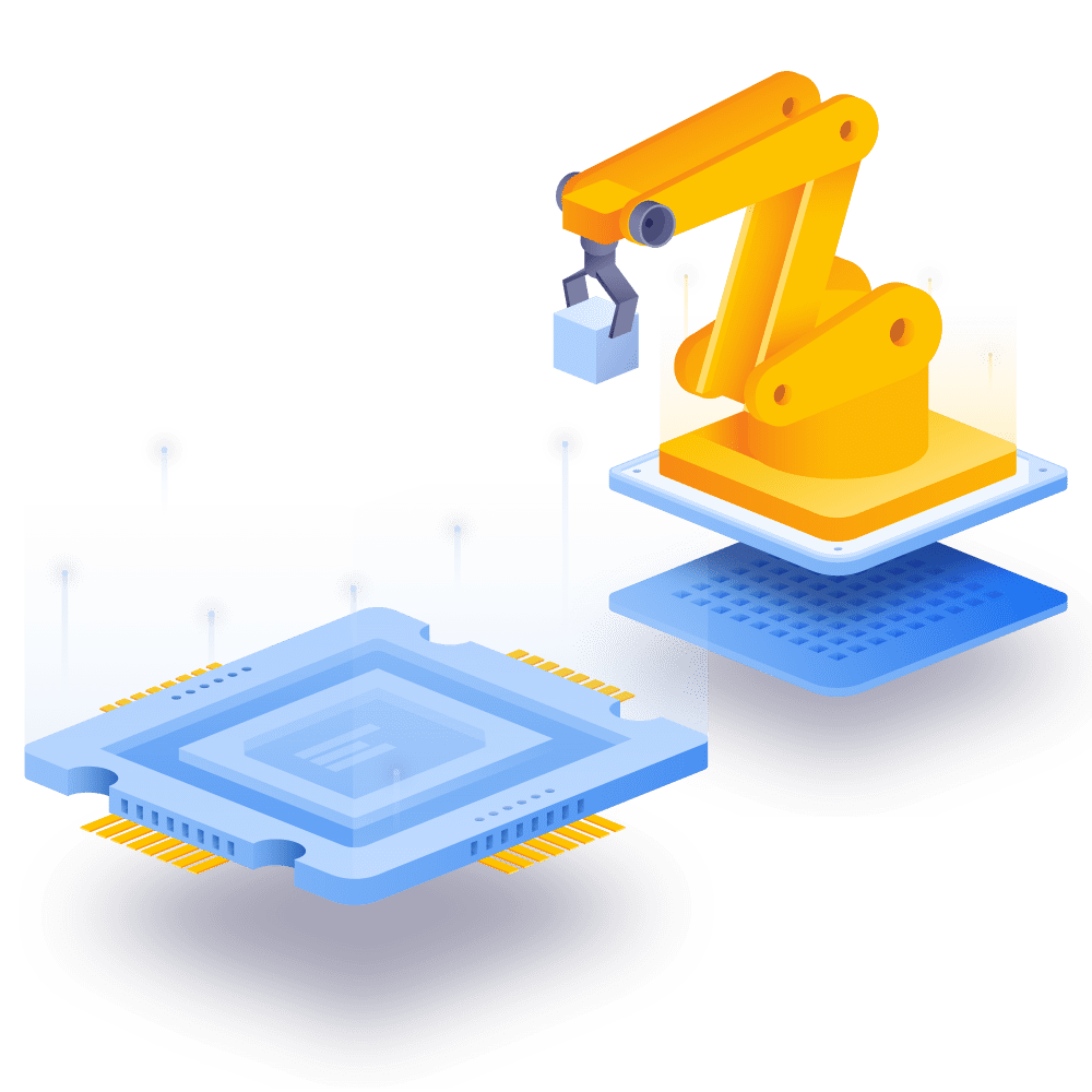
We listen to your needs and requirements in the fields of industrial precision mechanics and microelectronics.

Advice

Accompaniment
French sales force of the best international brands, we accompany you at all stages of your project, from design to after-sales service.
Mission
Serving businesses
ABAC International is the French business power for foreign companies specialized in industrial precision mechanics and microelectronics. As such we provide our French and French-speaking customers with access to these high value-added solutions.


Our expertise

Industrial Precision Mechanics
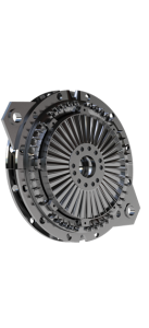
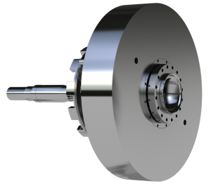
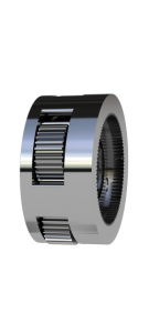
We offer industrial precision mechanic systems with great reliability for those industries which are the most demanding in terms of performance, lifespan and technical rigour.

Microelectronics
We offer state-of-the-art high-technology solutions to respond to your specific needs in extreme areas.

Online process
We offer state-of-the-art high-technology solutions to respond to your specific needs in extreme areas.

Our service
A global accompaniment
We offer our clients a global service which combines high standards and quality in professional relationships all through the commercial process and in product support.

ABAC International
Why choose us?

Find the best technical solution
Our technical knowledge, linked to a complete study of your expectations, allows us to propose better solutions, always respecting your design specification.

Win time
We will win you time in your business dealings thanks to favoured, long-established partnerships with suppliers, dealing with them in their mother tongue.

Simplifiy your supplier relationship
We provide French support for the best European brands. We simplify and faciltate your relationship with suppliers from the beginning of your project up to its completion.

Guarantee the best relationship between quality and price
Your will enter into direct contracts with the suppliers. Our commerical role is financed by major brands who guarantee you the best ratio quality/price.
THE QUALITY OF OUR BRANDS
A rigorous selection
ABAC International gives particular attention to its selection of commercial partners and proposed solutions.
Exceptional technological solutions
Our engineering teams develop extraordinary bespoke solutions, offering you the chance to modernize your industrial equipment and preserve your competitive advantage.
Cutting-edge production sites
Using cutting-edge technology, our factories allow you to benefit from solutions recognized throughout the world for their reliability.
Strenghtened quality controls

They trust us






News & Achievements
Installation by ACTEMIUM of a DESCH clutch-brake combination for a press upgrade
Business visits and technical exchanges alongside ACTEMIUM, initiated and accompanied by ABAC International, have allowed for the replacement of competitor equipment, on a forging press 2 500 tons, by a DESCH HKB clutch/brake combination hydraulically actuated. The...
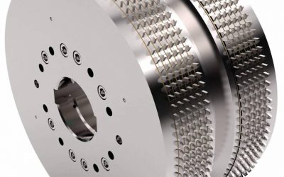
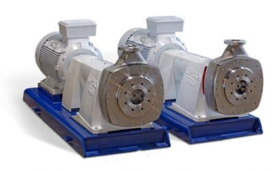
Modernization of production at BASF via the purchase of a SUPRATON homogenizer from Buckau-Wolf.
The client wanted to replace a homogenization equipment to optimize the production of a chemical base for healthcare products. The support of ABAC International has facilitated technical understanding by explaining the proposal of Buckau-Wolf for rotor/stator tools in...
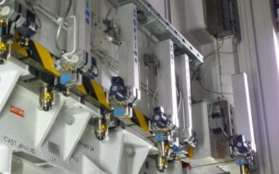
Renewal by OPTIMA of all clamping equipments on a VOLVO Truck press line
The relationship between the OEM and OPTIMA Spanntechnick, shaped and driven by ABAC International, has led to the replacement by OPTIMA of 64 clamping systems on a SCHULER hydraulic press line. The clamping elements need to be reliable for the tooling changes are...
Contact
Specific needs in industrial precision mechanics or microelectronics?
We have solutions for each of your needs.


